Abstract: The State Grid Smart Grid Research Institute, the Institute of Semiconductors of the Chinese Academy of Sciences, the Institute of Physics of the Chinese Academy of Sciences, Beijing Tianke Heda Blu-ray Semiconductor Co., Ltd. and other major projects of the Beijing Municipal Science and Technology Commission, "1200V/20A silicon carbide diode research and development" in 2015 3 Pass at the end of the month...
Led by the State Grid Smart Grid Research Institute, the Institute of Semiconductors of the Chinese Academy of Sciences, the Institute of Physics of the Chinese Academy of Sciences, Beijing Tianke Heda Blu-ray Semiconductor Co., Ltd. and other major projects of the Beijing Municipal Science and Technology Commission, "1200V/20A silicon carbide diode research and development" at the end of March 2015 Accepted by experts. Through the implementation of the project, the Beijing region has realized the localization of silicon carbide from the preparation of single crystal materials, the growth of epitaxial materials to the development of diode chips and its verification of power system applications, and the formation of an annual production capacity of 20,000 4 inch SiC wafers, 30 A 4 inch epitaxial wafer, an annual output of 100,000 SiC diodes and 10,000 silicon carbide modules in small batch production capacity, domestic silicon carbide devices have been initially verified by the application of photovoltaic inverters.

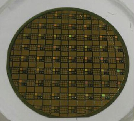
As a third-generation semiconductor material, silicon carbide has the advantages of large breakdown electric field strength, high thermal conductivity, wide band gap width and high melting point compared with silicon. It can be applied to power electronic devices to fundamentally improve the power conversion device. The efficiency, reduce the matching radiator and filter consumables, and also reduce the size of the equipment and improve the reliability of the equipment, so it has great application value in the field of high-end frequency conversion applications. In the organization and top-level design of the “1200V/20A Silicon Carbide Diode R&D†project, the Beijing Municipal Science and Technology Commission paid special attention to covering all the main links of the industrial chain from silicon carbide materials to devices and applications, integrating silicon carbide materials and epitaxy in Beijing. The superior resources of the device development and application unit, focusing on the technical research of silicon carbide single crystal substrate, epitaxial material, diode chip and module, photovoltaic inverter application, etc., finally successfully completed the localization research in this field and realized a small Batch production capacity.
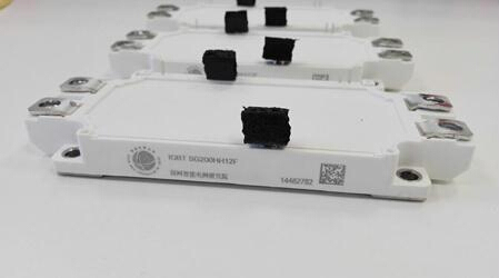
The project has accumulated 13 invention patents and published 8 scientific papers, including 4 SCI searches. The implementation of the project has greatly improved the overall design capability and manufacturing level of the domestic silicon carbide industry chain, promoted the development of the third-generation semiconductor materials and device industry, broke the monopoly of foreign technology, enhanced China's core international competitiveness and supported the implementation of energy-saving and emission reduction strategies. Important practical significance.
FRP Wave Roof Sheet
Frp Roof,Lightweight Roof Tiles,Frp Wave Roof Sheet,Fibreglass Roof Panels
PINGYUN INTERNATIONAL , https://www.pingyunconstruction.com